- 您现在的位置:买卖IC网 > Sheet目录1994 > DS3232MZ+ (Maxim Integrated Products)IC RTC W/SRAM I2C 8SOIC
DS3232M
±5ppm, I2C Real-Time Clock with SRAM
22
Maxim Integrated
slave address byte with R/W = 1, reads the data byte
with a NACK to indicate the end of the transfer, and
generates a STOP condition. However, since requir-
ing the master to keep track of the memory address
counter is impractical, use the method for manipulat-
ing the address counter for reads.
Manipulating the Address Counter for Reads: A
dummy write cycle can be used to force the address
counter to a particular value. To do this the mas-
ter generates a START condition, writes the slave
address byte (R/W = 0), writes the memory address
where it desires to read, generates a repeated START
condition, writes the slave address byte (R/W = 1),
reads data with ACK or NACK as applicable, and
generates a STOP condition. See Figure 6 for a read
example using the repeated START condition to
specify the starting memory location.
Reading Multiple Bytes from a Slave: The read
operation can be used to read multiple bytes with a
single transfer. When reading bytes from the slave,
the master simply ACKs the data byte if it desires to
read another byte before terminating the transaction.
After the master reads the last byte it must NACK to
indicate the end of the transfer and then it generates
a STOP condition.
Applications Information
Power-Supply Decoupling
To achieve the best results when using the DS3232M,
decouple the VCC and/or VBAT power supplies with
0.1FF and/or 1.0FF capacitors. Use a high-quality,
ceramic, surface-mount capacitor if possible. Surface-
mount components minimize lead inductance, which
improves performance, and ceramic capacitors tend to
have adequate high-frequency response for decoupling
applications.
If communications during battery operation are not
required, the VBAT decoupling capacitor can be omitted.
Using Open-Drain Outputs
The INT/SQW output is open drain and requires an exter-
nal pullup resistor to realize logic-high output level. Pullup
resistor values between 1kI and 10MI are typical.
The RST output is also open drain, but is provided with
an internal 50kI pullup resistor (RPU) to VCC. External
pullup resistors should not be added.
SDA and SCL Pullup Resistors
SDA is an open-drain output and requires an external
pullup resistor to realize a logic-high level.
Because the device does not use clock cycle stretching,
a master using either an open-drain output with a pullup
resistor or CMOS output driver (push-pull) could be used
for SCL.
Battery Charge Protection
The device contains Maxim’s redundant battery-charge
protection circuit to prevent any charging of the external
battery.
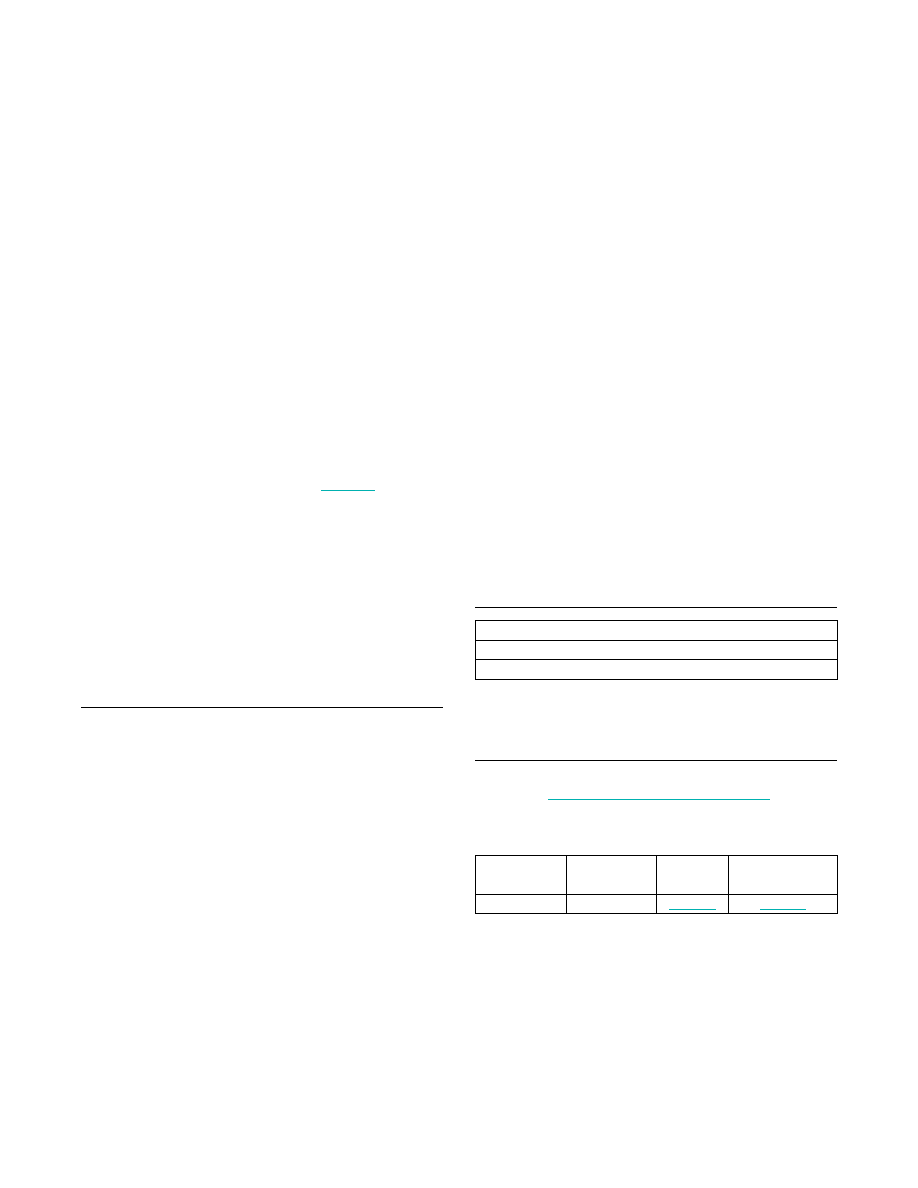
Ordering Information
Package Information
For the latest package outline information and land patterns (foot-
prints), go to www.maximintegrated.com/packages. Note that a
“+”, “#”, or “-” in the package code indicates RoHS status only.
Package drawings may show a different suffix character, but the
drawing pertains to the package regardless of RoHS status.
+Denotes a lead(Pb)-free/RoHS-compliant package.
/V denotes an automotive qualified part.
PACKAGE
TYPE
PACKAGE
CODE
OUTLINE
NO.
LAND
PATTERN NO.
8 SO
S8MK+1
PART
TEMP RANGE
PIN-PACKAGE
DS3232MZ+
-40NC to +85NC
8 SO
DS3232MZ/V+
-40NC to +85NC
8 SO
发布紧急采购,3分钟左右您将得到回复。
相关PDF资料
DS3232SN#T&R
IC RTC W/TCXO 20-SOIC
DS3234S#
IC RTC W/TCXO 20-SOIC
DS32C35-33#T&R
IC RTC ACCURATE I2C 3.3V 20-SOIC
DS3911T+
IC DAC 10BIT I2C QUAD 14TDFN
DS4000KI/WBGA
IC OSC TCXO 19.44MHZ 24-BGA
DS4026S+WCN
IC OSC TCXO 25MHZ 16-SOIC
DS4100HW+
IC OSC CLOCK 100MHZ 10LCCC
DS4266P+
IC OSC CLOCK 266MHZ 10-LCCC
相关代理商/技术参数
DS3232MZ+TRL
功能描述:实时时钟 RTC/TCMO/MEMS RoHS:否 制造商:Microchip Technology 功能:Clock, Calendar. Alarm RTC 总线接口:I2C 日期格式:DW:DM:M:Y 时间格式:HH:MM:SS RTC 存储容量:64 B 电源电压-最大:5.5 V 电源电压-最小:1.8 V 最大工作温度:+ 85 C 最小工作温度: 安装风格:Through Hole 封装 / 箱体:PDIP-8 封装:Tube
DS3232N
制造商:MAXIM 制造商全称:Maxim Integrated Products 功能描述:Extremely Accurate I2C RTC with Integrated Crystal and SRAM
DS3232S
制造商:Maxim Integrated Products 功能描述:Extremely Accurate I2C RTC
DS3232S-
制造商:MAXIM 制造商全称:Maxim Integrated Products 功能描述:Extremely Accurate I2C RTC with Integrated Crystal and SRAM
DS3232S#
功能描述:实时时钟 Integrated RTC/TCXO/Crystal RoHS:否 制造商:Microchip Technology 功能:Clock, Calendar. Alarm RTC 总线接口:I2C 日期格式:DW:DM:M:Y 时间格式:HH:MM:SS RTC 存储容量:64 B 电源电压-最大:5.5 V 电源电压-最小:1.8 V 最大工作温度:+ 85 C 最小工作温度: 安装风格:Through Hole 封装 / 箱体:PDIP-8 封装:Tube
DS3232S#T&R
制造商:Maxim Integrated Products 功能描述:EXTREMELY ACCURATE I2C RTC 20SOIC W - Tape and Reel 制造商:Maxim Integrated Products 功能描述:DS3232 3V 20P SOIC 制造商:Maxim Integrated Products 功能描述:IC RTC W/TCXO 20-SOIC
DS3232S#T&R
功能描述:实时时钟 Integrated RTC/TCXO/Crystal RoHS:否 制造商:Microchip Technology 功能:Clock, Calendar. Alarm RTC 总线接口:I2C 日期格式:DW:DM:M:Y 时间格式:HH:MM:SS RTC 存储容量:64 B 电源电压-最大:5.5 V 电源电压-最小:1.8 V 最大工作温度:+ 85 C 最小工作温度: 安装风格:Through Hole 封装 / 箱体:PDIP-8 封装:Tube
DS3232SN
制造商:Maxim Integrated Products 功能描述:Extremely Accurate I2C RTC